Cleanroom Access Opened – K76 Microelectronics & Semiconductor Physics Students at UTT Experience Advanced Chip Fabrication Technology at NACENTECH
On April 24, 2026, students of Class K76 majoring in Microelectronics and Semiconductor Physics, Faculty of Applied Sciences, University of Transport Technology (UTT), participated in a practical learning program at the National Center for Technological Innovation (NACENTECH). Instead of approaching knowledge through traditional methods, the visit provided students with a direct understanding of how semiconductor technology operates in real-world environments.
.jpg)
During the program, students were comprehensively introduced to the operational conditions of semiconductor fabrication, from technical systems to technological processes. Under the guidance of engineers, they gradually gained a clearer understanding of how a high-tech environment is established and operated in accordance with strict standards.
In particular, the content on cleanrooms—the core element in microchip manufacturing—left a strong impression. A cleanroom is an enclosed space where factors such as dust, temperature, humidity, and pressure are strictly controlled to meet required cleanliness standards. This is a mandatory condition in semiconductor production, as even minor environmental deviations can significantly affect product quality.
(4).png)
Within the program, students were guided by technical staff to observe external cleanroom systems, including gas, water, temperature, and humidity control systems—fundamental components of the entire production process. In addition, representatives of the Institute introduced typical semiconductor components researched and manufactured by NACENTECH, providing students with a clearer understanding of real-world industry products.
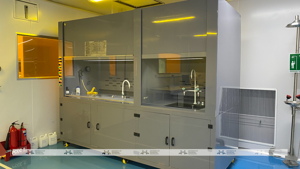
A highlight of the program was the opportunity for students to directly enter the cleanroom area to observe the operation and testing of specialized equipment. This hands-on experience not only enhanced practical understanding but also enabled students to clearly visualize how a semiconductor fabrication line operates under strict standard conditions—something that classroom learning alone cannot fully replicate.
.jpg)
Through this study visit, K76 students initially grasped key concepts of cleanroom operation and semiconductor fabrication processes, while also becoming familiar with professional working styles in laboratory and high-tech environments. These direct experiences helped bridge the gap between theory and practice, thereby strengthening students’ professional competencies.
.jpg)
Although the program has concluded, its impact extends beyond immediate knowledge and experience. Direct exposure to cleanroom environments—still relatively limited in Vietnam—has enabled students to better understand the practical requirements of the industry, fostering a serious learning attitude and long-term career orientation. This serves as an important foundation for students to confidently enter the field of microelectronics and semiconductors with solid knowledge and an adaptive mindset toward modern technologies.
.png)


